中 文 版
English
Home
About Us
Research
People
Facilities
Training
User Guide
Contact Us
Facilities
●
Micro/nano Fabrication
> He/Ne-ion Microscope
> DTL UV Litography
> DWL 66+
> EBL Raith 150
> EBL JBX-6300FS
> FIB/SEM DB235
> FIB/SEM Helios 600i
> UV Mask Aligner MA6
> 3D DLW
> Nano Imprint
> Laser Interference Lithography
●
Dry Etching
> RIE Plasma80
> RIE NGP80
> Ion Beam Etching
> ICP Plasma100
> ICP Cobra
> Microwave Plasma
●
Materials Growth
> TED DZ-300
> EBD FU-12PEB
> Thermal Evaporator
> Atomic Layer Deposition
> Electron Beam Evaporator
> UHV Thin Film Deposition
> MPCVD
> PECVD
●
Charactorization
> SNOM
> Nano Indenter
> AFM
> Dual Probe SEM
> AFM/MFM
> PPMS
> Surface Profiler
> Ellipsometer
> Electro-chemical Stat.
> 3D Surface Analyzer
> Probe Stage
●
Auxiliary
> Wire Bonder
> Rapid Annealing Process
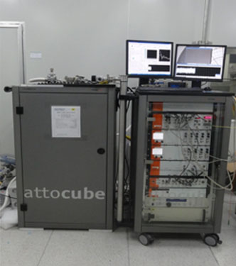
扫描近场光学显微镜
Customized attoLIQUID-9T attoSNOM III & CFM Microscope
Lowest temperatures:1.8 K
Magnetic Field:9T @4.2K
Laser:630nm /1300nm
SNOM resolution:<200 nm
CFM resolution:<650nm
Contact person:
Shibing Tian
Techniques and Applications:
It can be used to directly observe the surface structure of nanostructures, and observe the near-field interaction between the incident light and the nanostructure under different low temperature and strong magnetic field environments.