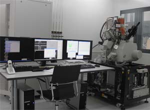
Focused Ion Beam Microscopy FEI Helios 600i
Technical specifications and key features:
High resolution FESEM
High performance Ga+ Source column
CrossBeam® operation: high resolution imaging and milling/polishing
Optional multi-channel GIS: Pt, W, XeF, I2
Sample size: up to 2 inches
Image archiving, networking and hardcopy solutions from the integral Windows® operating system
Resolution: SEM: ≤ 0.9nm @ 15kV;≤ 1.4nm @ 1kV; FIB: 2.5nm @ 30kV
Probe Current: SEM: 4 pA - 20 nA; FIB: 1 pA - 65 nA
Acceleration Voltage: SEM: 350 V - 30 kV; FIB: 500 V - 30 kV
Emitter: SEM: Thermal field emission type; FIB: Ga LMIS
Sample size: up to 2 inches
Contact person:Wuxia Li
Techniques and Applications:
FIB Helios 600i is capable of fabricate structures with feature size down to 10 nm by both low current etching and GIS assisted deposition, in the construction of micro-/nano electronic devices, optic-electronic devices, bio-sensors/channels, MEMS/NEMS, superconducting/magnetic devices, photonic crystals, plasmonic devices and so on, as well as to explore the novel physic phenomena and effects in nanometer scale. It can also be used to fabricate TEM cross-section for atomic scale analysis, with much increased material removal speed as well as much reduced damages and contaminations using the very low current polishing and imaging. In addition, the system is equipped with nano-manipulators for in-situ object transfer.