

2015.2.9
Scientists from the LMF have published a simply reproducible high-throughput approach to fabricate feasibly a double-layer stacked Au/Al2O3@Au nanosphere structures on silicon wafer by by rapid thermal annealing (RTA) and atomic layer deposition process (ALD), to bring high density, high intensity “hot spots” effect. These wafer-scale, high density homo/hetero-metal-nanosphere arrays with tunable nanojunction between adjacent shell-isolated nanospheres have significant implications for ultrasensitive Raman detection, molecular electronics, and nanophotonics.
The scientists have shown that the double-layer stacked Au nanospheres construct a three-dimensional plasmonic nanostructure with tunable nanospacing and high-density nanojunctions between adjacent Au nanospheres by ultrathin Al2O3 isolation layer, producing highly strong plasmonic coupling so that the electromagnetic near-field is greatly enhanced to obtain a highly uniform increase of SERS with an enhancement factor (EF) of over 107 . Both heterogeneous nanosphere group (Au/Al2O3@Ag) and pyramid-shaped arrays structure substrate can help to increase the SERS signals further, with a EF of nearly 109 .
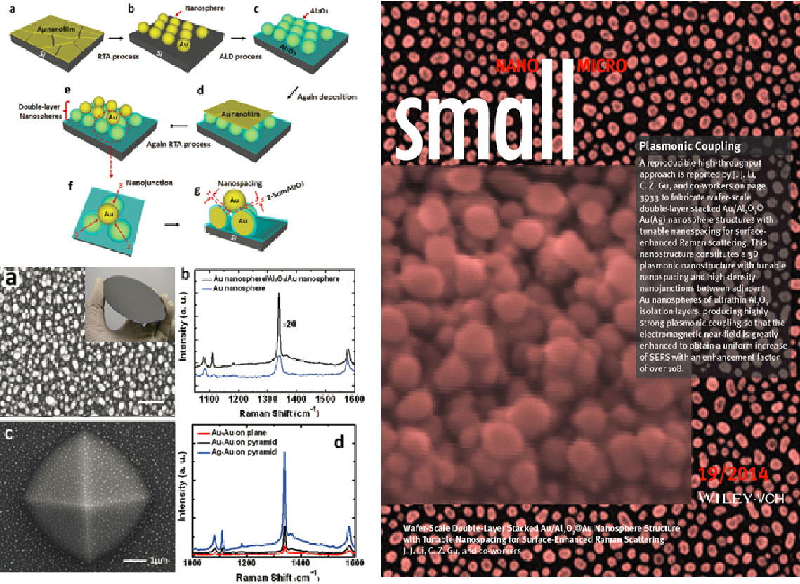
Image: Double-layer stacked Au/Al2O3@Au nanosphere structures and its SERS properties
Original article: Z. Hu et al (2014) “Wafer-Scale Double-Layer Stacked Au/Al2O3@Au Nanosphere Structure with Tunable Nanospacing for Surface-Enhanced Raman Scattering small 2014, 10, No. 19, 3933–3942.